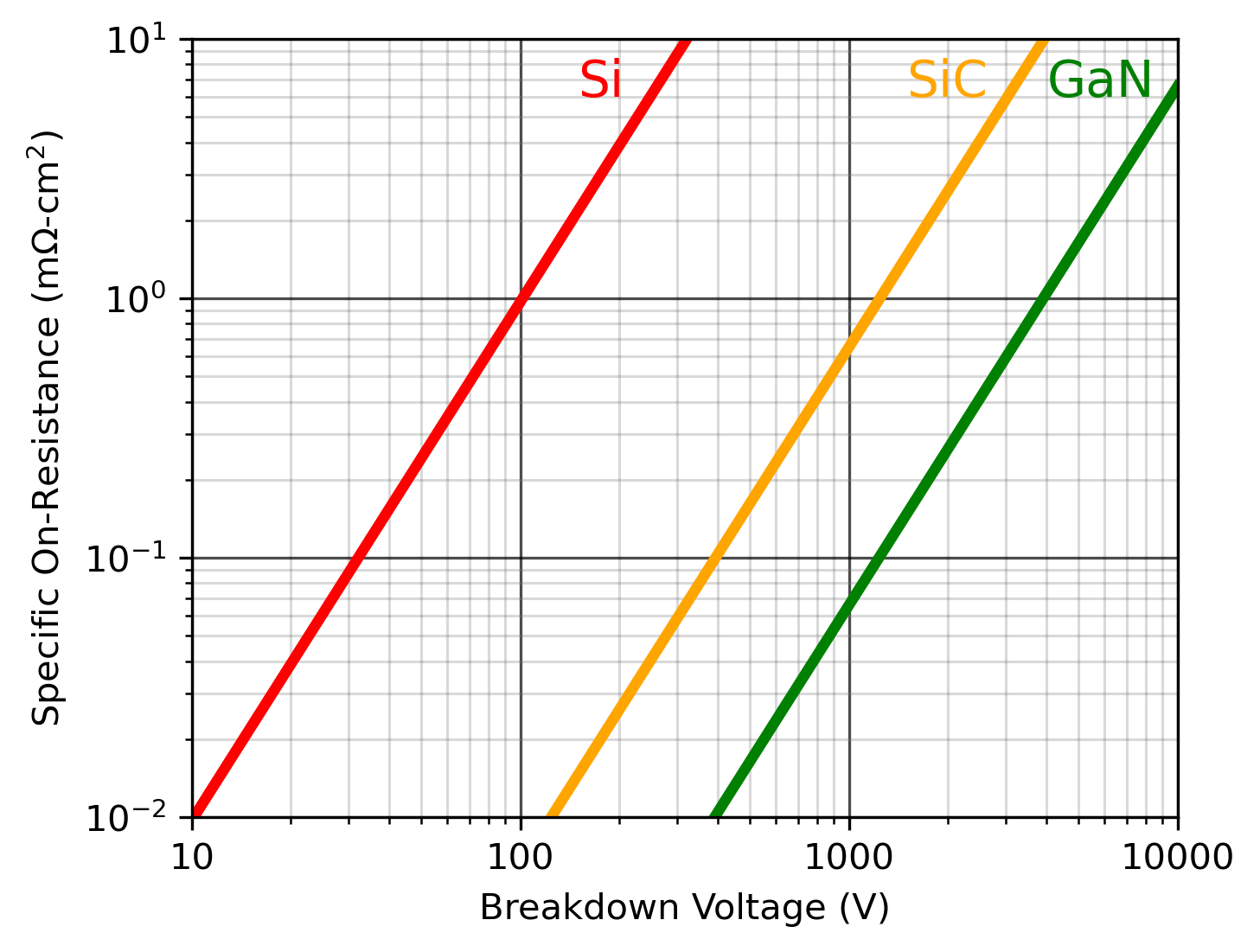
Gallium nitride (GaN) based power-switching transistors are superior to their silicon (Si) and silicon carbide (SiC) counterparts due to materials properties which allow for significantly smaller wafer area devices with equivalent breakdown voltage, on-resistance, and current handling capability to be realized.
Comparison of specific on-resistance limits at breakdown voltages from 10-10,000 V of Si, SiC, and GaN.
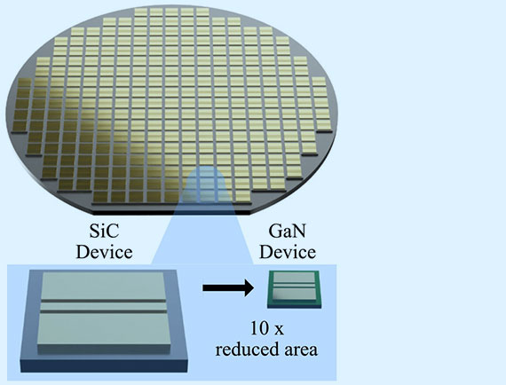
Wafer of power-switching transistors and a comparison of SiC and GaN device sizes
GaN devices have the same current handling capacity, breakdown voltage, and on-resistance as SiC devices, but take up 10x less wafer areas
The devices are cheaper to produce as they make more area-efficient use of wafers
Importantly, the devices have ~10X less capacitance, which greatly increases the switching speed of converter circuits using these parts
Making a difference to "Switch-Mode" power converters
“Switch-Mode” power converters are a broad class of power conversion circuits used to convert electrical power from one form to another. The applications include consumer electronics, electric vehicles, solar photovoltaics, and smart power grid distribution applications. At the heart of every power converter, is the semiconductor power switch. This component determines the performance of the whole system. Currently, the dominant power switching semiconductor material used is Si, with high-performance applications making use of SiC due to its superior materials properties.
The physical size of a power conversion system is inversely proportional to its operating frequency due to the size of the passive components shrinking with increasing operating frequency. The operating frequency is dictated by the limitations of the semiconductor power switch. Since GaN switches allow for switching speeds ~10X greater than SiC switches, GaN-based power converters are considerably smaller than SiC-based systems: ~1/4 the volume and weight. These systems are not only smaller and lighter, but importantly, cheaper to produce as the cost of passive components roughly scales with size and weight as well.
Vertical-Conduction over Horizontal-Conduction Devices
Gallium nitride (GaN) based power-switching transistors are superior to their silicon (Si) and silicon carbide (SiC) counterparts due to materials properties which allow for significantly smaller wafer area devices with equivalent breakdown voltage, on-resistance, and current handling capability to be realized.
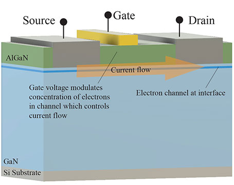
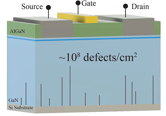
GaN HEMT device. Structure has no impurity doping. Well-developed radio frequency transistor adapted for use in power-switching applications.
HEMTs have all the device contacts on the surface of the wafer. Current flow is along a channel which is formed at the interface between AlGaN and GaN. The structure is well-known and the technology around it well developed. It has the advantage that there are no regions of impurity doping needed – something which is very difficult to achieve in GaN. In this type of device the electron channel that forms at the interface of the AlGaN and GaN does so due to the difference in polarization of AlGaN and GaN. This type of device is “normally-on” as in, current is allowed to flow from the source to drain until a bias voltage is placed on the gate to stop it.
This is undesirable from both a safety and compatibility standpoint, and most devices of this type are paired with a Si transistor to make them “normally-off” to be appropriate for power switching applications.
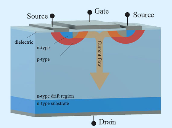
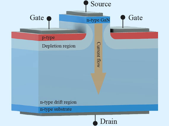
Si and SiC-based power transistors are all of the vertical-conduction geometry. These device geometries rely on what is known as impurity doping to achieve the area-selective p-type regions employed in the device. They are normally-off devices, meaning no current flows unless a bias is applied to the gate terminal.
Vertical-conduction power-switching devices. These devices all rely on area-selective impurity doping. They are normally-off devices.
This geometry of vertical-conduction devices is favorable as it makes area-efficient use of the substrate, allows for a normally-off device, and also provides isolation of high voltages that exist between terminals. All high voltage power transistors made of Si and SiC take one of these two forms.
The Odyssey Edge
Starting a revolution without reinventing the wheel
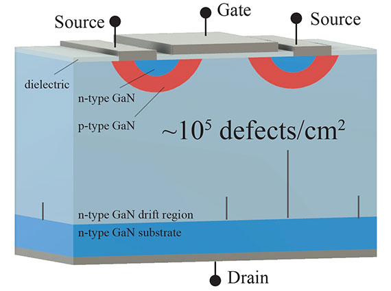
Odyssey Semiconductor has developed a revolutionary method to achieve area-selective doped regions in GaN, opening the door to the realization of vertical-conduction devices analogous to the highly developed device geometries that are standard in Si and SiC – but with all the superior materials properties of GaN.
Defects Matter
Horizontal-conduction GaN HEMTs are grown Si wafers. Since the current flows in and out of contacts on the surface, the choice of substrate is not constrained as it is not in the path of current flow. This is an advantage in that Si is cheap, and wafers are available in large format. The disadvantage is that when growing any semiconductor on top of a dissimilar semiconductor, vast amounts of crystal defects are introduced in the crystal layer grown. For GaN grown on Si, the defect density is ~108 to 1010 cm-2. These defects interfere with the high voltage operational reliability of the devices. As a result, no GaN HEMTs have been commercially released with voltage ratings above 900 V and the majority are limited to ~650 V.
A high degree of interfacial defects limits reliable operating voltages to < 600-900 V.
Vertical-conduction devices require that the substrate be the same material as the drift region. For GaN, this requires a bulk GaN substrate. While expensive and not available in sizes larger than 100 mm, the bulk GaN substrates allow vertical-conduction GaN transistors to be made in material with defect densities ~103 to 105 cm-2. This low defect density allows GaN transistors to have high reliability at voltages far above 1,000 V.
Vertical-conduction GaN devices grown on GaN substrates have~1000-10,000 fewer defects per unit area allowing for reliable operation at voltages up to 10,000 V and beyond. The much smaller die size of the GaN devices makes them competitive to produce relative to SiC devices with similar ratings even though the GaN substrates are more expensive.
Odyssey Semiconductor is utilizing high-quality bulk GaN wafers as the substrate for their proprietary vertical-conduction power switching transistors. These substrates allow the growth of low defect density device layers needed for transistors with ratings above 1,000 V.
Operating Voltage that will drive the replacement of SiC Devices in power transistor applications
For many power transistor applications dealing with the conversion of AC voltages, the semiconductor part needs to have a voltage rating ~3X greater than the root mean square (RMS) AC voltage. Consumer electronics applications are around 120-240 V AC, electric cars currently operate at 400 V, and three-phase industrial applications operate at 480 V AC.
The HEMT-type 650 V rated horizontal-conduction devices are largely limited to consumer electronics applications dealing with the conversion of low voltage 120-240 V single-phase AC. Such as AC-DC power supplies for charging battery-powered electronics such as phones and laptop computers.
There is, however, a great need for increased efficiency in electric vehicles and industrial 480 V applications which are currently being served by SiC and Si power transistors since current GaN HEMT-type devices cannot operate at the voltages required of these applications. Successful realization of GaN transistors with ratings above 1,000 V will open the door to smaller, more efficient voltage conversion systems for these high voltage, high power applications.
While Odyssey Semiconductor’s proprietary vertical-conduction power switching transistors are capable of operating below 1,000 V, this market is well served by the GaN-on-Si HEMT devices currently available. Odyssey Semiconductor is targeting a much higher power device market that is currently being served by SiC, with the aim of replacing SiC devices altogether.